
Integrated Photonics Fabrication
Our process enables researchers and industrial professionals to rapidly prototype integrated photonic circuits. Devices are manufactured using a state-of-the-art 100 keV electron beam lithography system.
Learn More
X-Ray Optics
The highest quality x-ray optics with proven resolution, efficiency and reliability at low costs for soft and hard x-rays for ptychography, STXM, TXM and phase contrast imaging.
Learn More
Calibration Standards
The ANT calibration standard was designed for the highest resolution requirements of X-Ray imaging systems with nanoscale features. Available for both soft and hard X-Ray regimes, EUV and optical setups.
Learn More
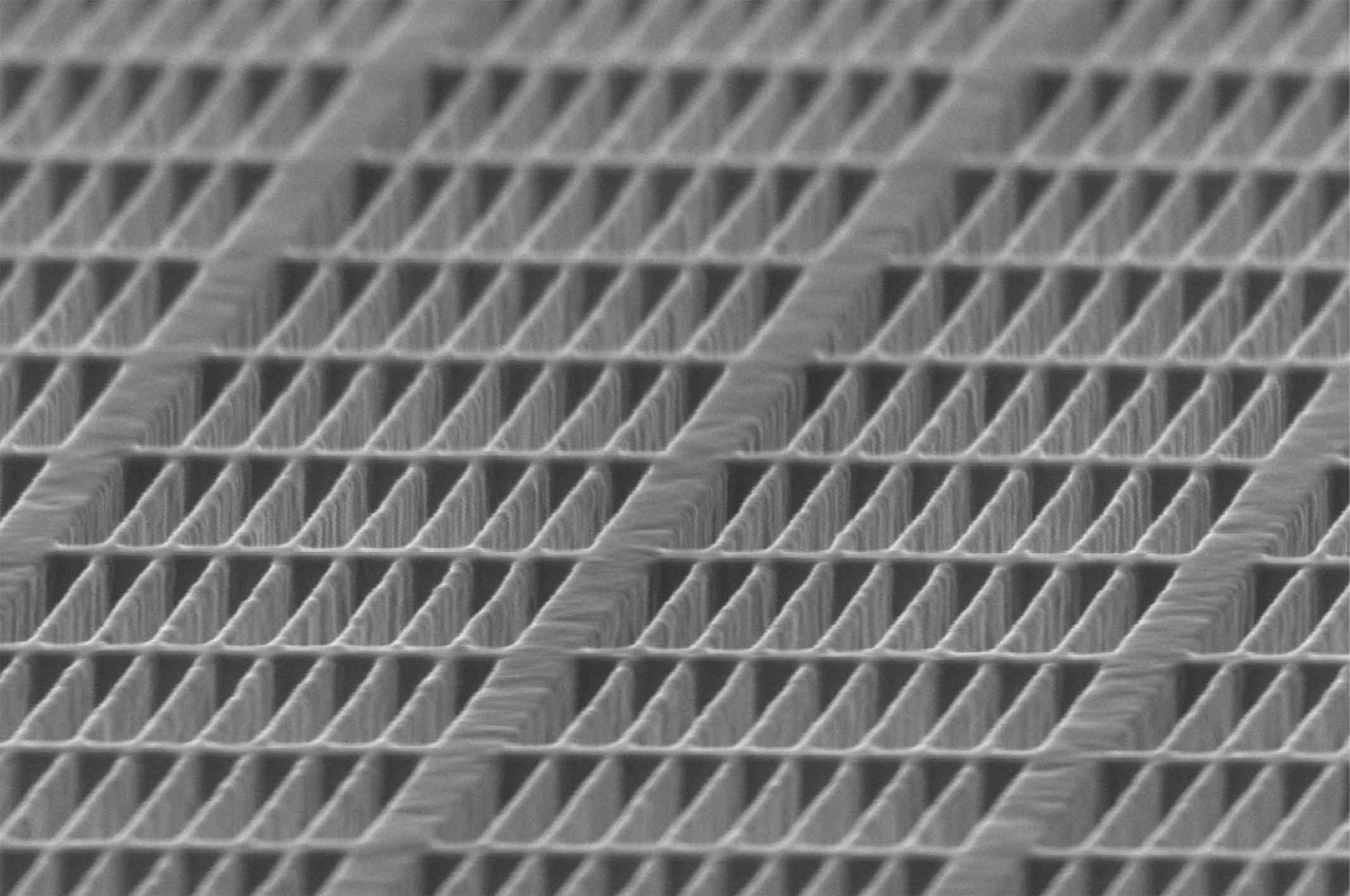
Gratings
Custom transmission gratings for EUV and higher energy X-ray systems. Our direct-write, fast through-put process allows for higher resolution gratings from several hundred micrometres to millimetres.
Learn More
Metalens Fabrication
Compact, lightweight, and high performance flat optical components with high-resolution subwavelength features in the visible and near-infrared spectra are manufactured using high throughput electron beam lithography.
Learn More



High Efficiency
We can fabricate your custom optic out of a variety of different materials to maximize the efficiency
High Resolution
We use the latest in electron beam lithography technology to pattern features down to 10 nm
Low Cost
With the most common zone plate specifications kept in stock and custom optics that are made to order we can deliver the highest quality with low costs
Fresnel Zone Plates
Zone plate optics for ptychography, phase contrast, and scanning microscopy in soft and hard X-ray regimes
High Resolution
Our calibration standards can be fabricated to have features as small as 12 nm
Custom Designs
Using state of the art electron beam technology to pattern designs we can put your logo onto our standard layout or your own custom layout
X-Ray, EUV and visible light
We can fabricate our calibration standards with a variety of feature sizes and various substrates related to the imaging application.
Calibration Targets
The ANT calibration standard was designed for the highest resolution requirements of X-Ray imaging systems with nanoscale features. Available for both soft and hard X-Ray regimes, EUV and optical setups.
High Resolution
We have the capability to pattern lines down to a resolution of 20 nm half pitch or 50,000 line pairs/mm (lp/mm).
High aspect ratio
Custom Applications
Our custom gratings can be used in synchrotron and lab-based systems for a range of applications. Contact us for more details for your specific needs
Gratings
Custom transmission gratings for EUV and higher energy X-ray systems. Our direct-write, fast through-put process allows for higher resolution gratings from several hundred micrometres to millimetres. Various metals can be fabricated on thin membranes of Si3N4, SiC, or Si.
Multi-Project Wafer Runs
Standard options include cladding oxide, metallization, and edge couplers.
Custom Dedicated Runs
Fully customized to suit your needs with many options available.
Rapid Fabrication
Turnaround time from design submission to delivery as short as three weeks.
Integrated Photonics
We are an integrated photonics foundry specializing in rapid turnaround prototyping and low-to-mid volume production. By using state-of-the-art electron beam lithography, we achieve features sizes of 60 nm. Our online design submission system is user-friendly and we offer a process design kit for our fabrication service.
High Resolution
Electron beam lithography patterning allows features as small as 100 nm.
Custom Dedicated Runs
An array of process customization options are available to suit your meta-optics needs.
Rapid Fabrication
Turnaround time from design submission to delivery in as little as eight weeks.
Metalenses
Applied Nanotools’ metalens foundry specializes in rapid turnaround prototyping and low-to-mid volume production. By using direct write electron beam lithography, we achieve feature sizes down to 100 nm to accommodate many applications for flat optics. While our standard meta-optical elements are composed of amorphous Si on fused silica substrates, other various materials may be used.