Metalens Foundry Service
Fabrication of metaoptics with rapid turnaround times
Rapid fabrication service for prototyping metalenses and metasurfaces
The Metalens Foundry Service is an extension of our NanoSOI Fabrication Service that specializes in the fabrication of metalenses and metasurfaces. Using state-of-the-art, high-throughput electron beam lithography, our foundry can manufacture various meta-optical elements comprised of high resolution subwavelength features with superior line-edge roughness and negligible stitching errors. Our anisotropic plasma etch process provides structures with high aspect ratios and smooth sidewalls, which translates to flexible metalenses with exceptional performance efficiency. Optional standard process steps such as oxide cladding deposition are available for our metalenses. Custom substrate material options are also available upon request to accommodate a wide array of applications.
The Metalens Foundry Service is accessible through custom dedicated runs, which offer metaoptic fabrication with a variety of personalized options. Timelines for these runs are flexible, and quotations are customized by our staff for each run. Multi-project wafer (MPW) runs, which batch design submissions from multiple users onto a single wafer fabricated under a standard set of design rules, will be available as of February 2026.
Looking for metalens fabrication services?
Please contact our support line to inquire about our metalens foundry service. We are happy to discuss pricing, design conception and verification, online design submission, and many other topics with you regarding metaoptics.
High quality metalens foundry for rapid-prototyping and high-resolution structures
Metaoptics can be made for visible (VIS) and near-infrared (NIR) wavelengths with different available materials.
|
Material |
Wavelength |
Thickness* |
|---|---|---|
| Amorphous Silicon | NIR | 760 nm |
| Niobium Oxide^ | VIS | 700 nm |
*Custom thicknesses available on dedicated runs.
^Currently only available on dedicated runs.
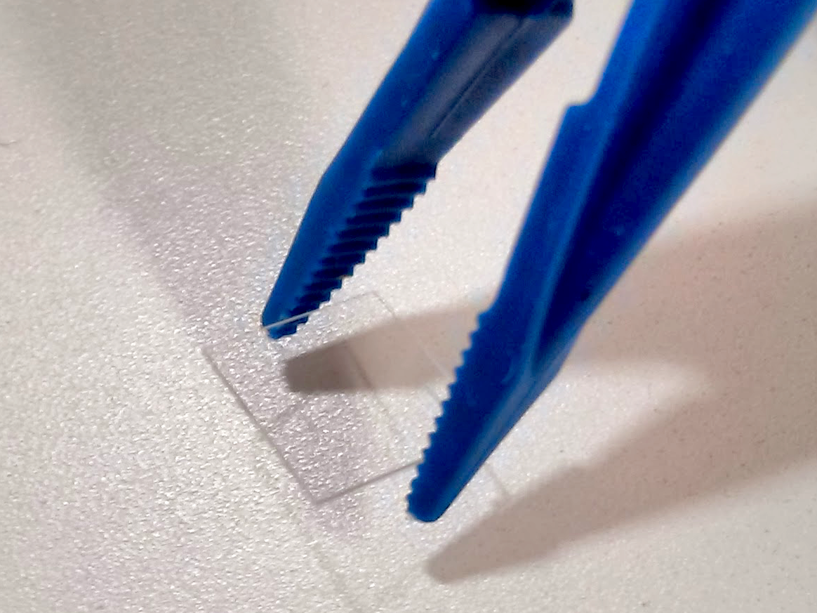
Fused silica substrates are the primary option for our metalenses, enabling excellent transparency of VIS and NIR light and a high quality substrate that is compatible with various metaoptic materials. For MPW runs, fused silica substrates have 500 μm thickness and dimensions of 1 cm x 1 cm. The substrate material and geometric specifications can be customized on dedicated runs.
Available Process Options
Several of these processes are available in multi-project wafer (MPW) runs and dedicated runs; some are available only in dedicated runs.

Silicon Device Layer
Feature sizes as small as 120 nm (aspect ratios ~ 6.3:1) with high performance electron beam lithography. Available in MPW and dedicated runs.
Our silicon patterning process involves the definition of metaoptic structures with nano-scale features in amorphous silicon (a-Si) using state-of-the-art, high-throughput electron beam lithography (EBL) and reactive ion etching (RIE) processes.
The patterning process begins by cleaning and spin-coating a material that is sensitive to electron beam exposure. A device pattern is defined into this material using 100 keV EBL. Once the material has been chemically developed, an anisotropic ICP-RIE etching process is performed on the substrate to transfer the pattern into the underlying a-Si layer. The etch is performed until there is no remaining silicon and the underlying silica layer is exposed.
The process produces compact, lightweight, high-quality metaoptics with small form factor in various quantities for a variety of applications in communications, computing, imaging, and sensing.
For MPW runs, the substrate consists of a 760 nm a-Si device layer on a 500 µm fused silica handle wafer. The a-Si device layer thickness and wafer specifications can be customized on dedicated runs.

Oxide Coating (Protective)
Cladding oxide to protect metalens integrity and enhance device performance. Available in dedicated runs.
If the metaoptic devices require isolation from the outside environment, silicon dioxide cladding can be deposited using chemical vapour deposition (CVD). Our standard oxide cladding thickness is 2.2 µm, but thickness of the protective film can be customized upon request.


Other Dedicated Run Options
These options are available in dedicated runs only.
In addition to the other process options listed here, we have many other custom options available for dedicated runs. Some examples include:
- Variable amorphous silicon device layer thickness
- Other metalens material options, such as niobium oxide for visible light metaoptics
- Custom substrate material options and geometric specifications (e.g., thickness, chip dimensions, etc.)
For the full list of our available processes, please click the button below to view our dedicated run information at the NanoSOI Design Center.
