Silicon Nitride Design Rules and Area
Design Rules
The following table summarizes the design rules for each layer available in the NanoSOI Silicon Nitride MPW runs:
| Layer Number | Process | Minimum Feature Size | Minimum Feature Spacing | Design Area | Notes |
|---|---|---|---|---|---|
| 4 | Silicon nitride full etch | 120 nm | 120 nm | 9 mm x 9 mm | Feature sizes specified where duty cycle of surrounding region is ≤ 50%. See example here. |
| 6 | Through-cladding windows | N/A | N/A | Standard layout is 9 x 9 mm. Deep trench layout is 8.78 x 8.78 mm | Requires prior approval to use. Please inquire with Support two weeks before MPW deadline. |
| 11 | Tri-layer metal: TiW alloy | 5 μm | 5 μm | Standard layout is 9 x 9 mm. Deep trench layout is 8.745 x 8.745 mm | -- |
| 12 | Tri-layer metal: TiW/Au Bilayer | 10 μm | 10 μm | Standard layout is 9 x 9 mm. Deep trench layout is 8.745 x 8.745 mm | -- |
| 13 | Tri-layer metal: Bond pad open | 10 μm | 10 μm | Standard layout is 9 x 9 mm. Deep trench layout is 8.745 x 8.745 mm | Must be placed over Layer 12 and smaller than Layer 12 by 5 μm. |
| 189 | Custom dicing | 100 μm | 3 mm | 9 mm x 9 mm | 50 μm spacing to devices. See example here. |
| 200 | SEM imaging | 500 nm wide | None | 9 mm x 9 mm | Only rectangular boxes with aspect ratio 4:3 (width to height). See example here. |
| 201 | Deep trench | 260 μm | 3 mm | 8.78 mm x 8.78 mm | 35 μm spacing to metal. Only extend Layer 4 edge couplers into Layer 201. See examples here and here. |
| 202 | Deep trench exclusion layer | 3 mm x 200 μm | 3 mm | -- | Required for deep trench layouts. Exclusion layer to allow for chip handling. See example here. |
| 203 | Thermal isolation trenches | 30 μm | 35 μm | 8.78 mm x 8.78 mm | 35 μm spacing to metal. 30 μm spacing to silicon nitride. See example here. |
| 998 | Dream Photonics FaML (reserved) | -- | -- | 8.78 mm x 8.78 mm | May only be used for Dream Photonics black box cells. White box cell replacement by ANT is only available for FaML cells. Please inquire with Support two weeks before MPW deadline. |
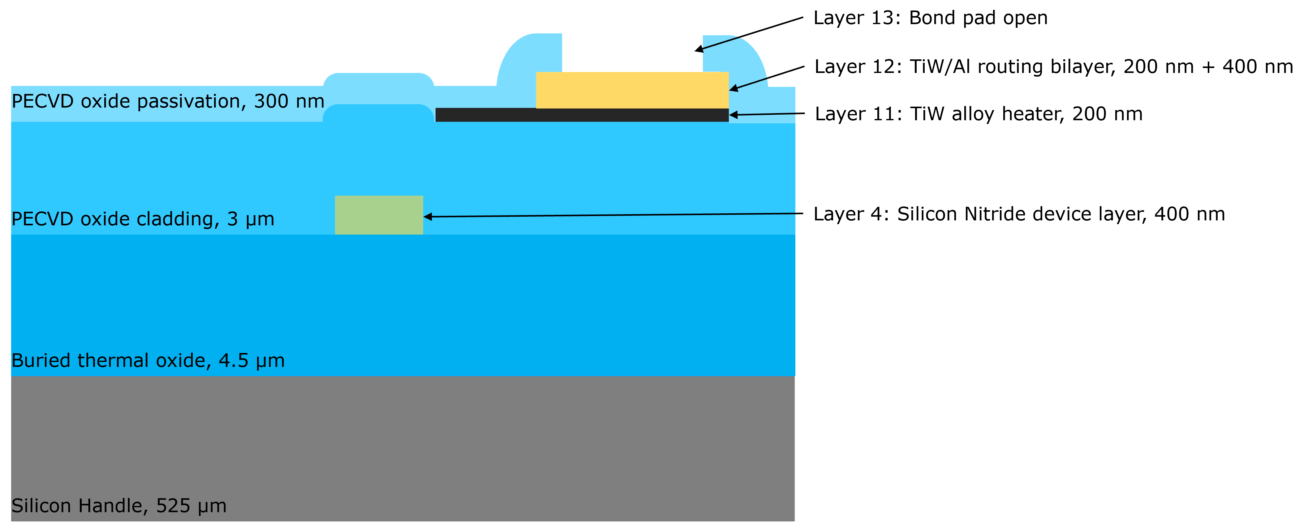
The image above shows the correlation of the layer numbers to each physical layer in the fabrication process. A layer definition file containing the NanoSOI layer information is available for download below. You can import the layer definition file into KLayout by choosing File, then Load Layer Properties. Design examples for deep trench, thermal isolation trenches, and the SEM imaging layer are also available. All of our tutorials are designed to match the Layer Definition file.
Download Layer Definitions
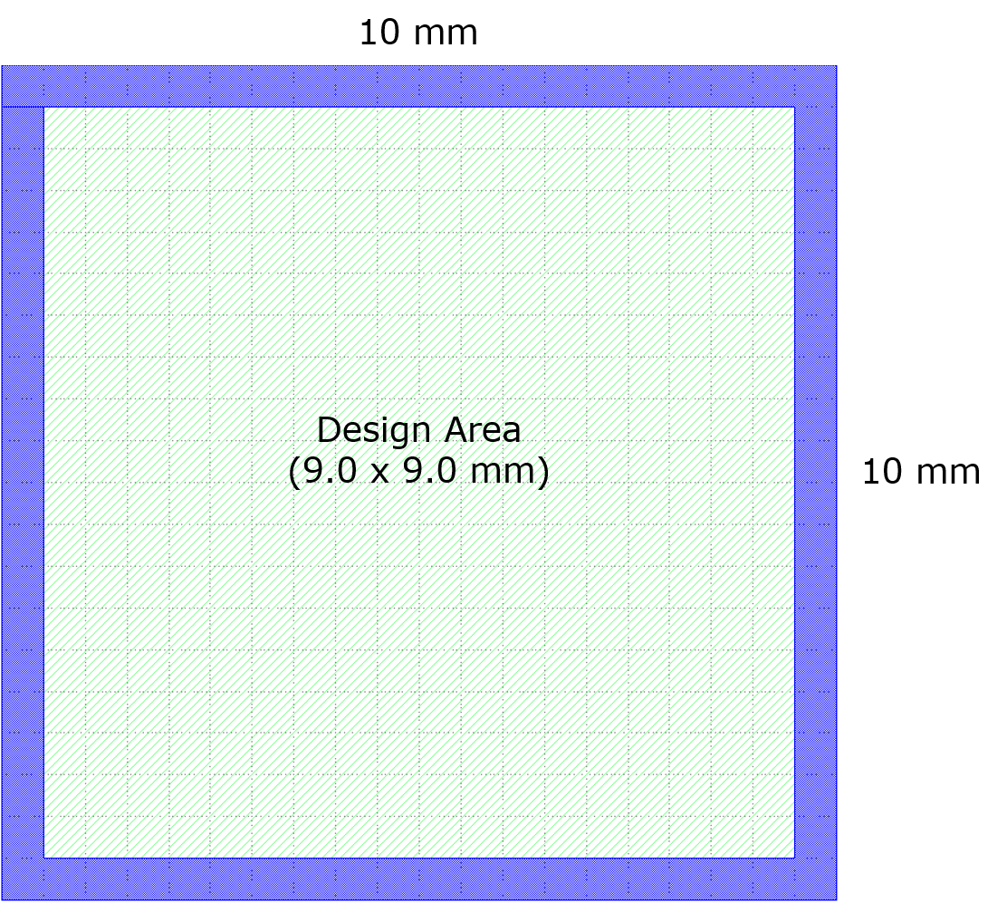
Physical Chip Size and Design Area
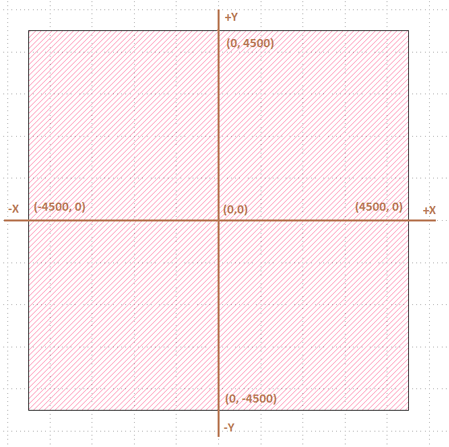
In our MPW runs, chips are fabricated on larger substrates, then singulated into individual chips with a physical footprint of 10 mm x 10 mm. The space reserved for your actual design is a 9.0 mm x 9.0 mm area. The placement of this bounding box is at the origin (x=0, y=0) of the GDSII design and extends to -4500 and +4500 in X/Y as shown below: