Process Overview
Silicon Nitride Device Layer
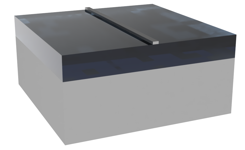
The foundation of the NanoSOI fabrication process is the device layer. Photonic waveguides capable of light propagation are patterned using 100 keV electron beam lithography technology. Fully-etched devices (etched down to the buffer oxide, as shown in the above diagram) are created using an e-beam mask material and anisotropic ICP-RIE etching process. The minimum feature size is 120 nm and the minimum feature spacing is 120 nm, where duty cycle of surrounding region is ≤ 50%. For duty cycles greater than 50%, resolution will decrease further because of proximity effects.
Silicon Nitride Substrate Specifications
| Device Layer Type | Device Layer Thickness | Buffer Oxide Layer Thickness | Silicon Handle (Substrate) Thickness | Wafer Manufacturer |
|---|---|---|---|---|
| Silicon nitride (SixNy) | 400 nm | 4.5 μm | 525 μm | Applied Nanotools fabricates the SixNy on WaferPro wafers |
Propagation Loss Measurements:
Applied Nanotools and its collaborators measure the optical propagation loss using microring resonators and extracting the round-trip loss from the measured optical spectra. The latest propagation loss results for fully-etched 400 nm silicon nitride waveguides is listed in the table below (publication of detailed data is pending):
| Waveguide Width | Waveguide Loss (1310 nm) | Waveguide Loss (1550 nm) |
|---|---|---|
| 0.75 μm | 0.8 dB/cm | 1.2 dB/cm |
| 1 μm | N/A | 1.0 dB/cm |
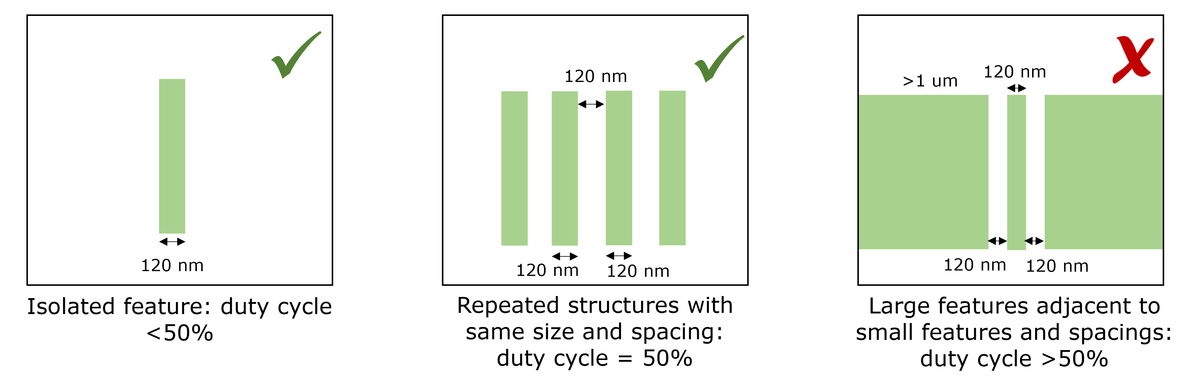
Proximity Effects:
A limitation of electron beam lithography technology is electron scattering effects when exposing patterns into the mask. During the file preparation process, we apply a proximity effect correction algorithm to the design to mitigate these effects. However, extreme cases such as large areas/pads (> 10 × 10 μm) in close proximity to high-resolution features or small feature spacings are difficult to correct for. Please inquire with us if your design has large areas to be exposed in conjunction with high resolution features or small spacings. For regions with duty cycle (pattered area ÷ total area) larger than 50%, the minimum dimension and minimum spacing will be larger than what is specified in the design rules. The examples below show acceptable designs (green check mark) and designs with duty cycles greater than 50% (red X).
Sidewall Angle:
Imperfections in the mask and the etching process will create an angle to the sidewall of the waveguide. As of November 2025, the sidewall angle of silicon nitride waveguides fabricated with our process is approximately 90 ± 2 degrees (improved from 83.5 degrees). The angle is also dependent on the density of the features and may vary slightly in areas with small gaps between features. We aim to have the waveguide dimensions match the GDS design with proximity and etch bias corrections applied during layout processing.
Oxide Cladding
A cladding oxide can be deposited onto silicon nitride devices. The deposition is performed using plasma-enhanced chemical vapour deposition (PECVD). The standard oxide deposition thickness for silicon nitride MPW runs is 3 µm, which is designed to optically isolate the waveguides from heaters deposited with the tri-layer metal process and improve edge coupler performance.
Thinner custom oxide cladding can be requested on dedicated runs. Please contact support@appliednt.com to inquire.
Tri-Layer Metallization
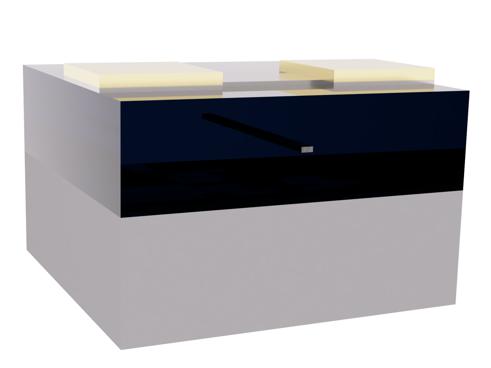
*Protective oxide layer not shown
The purpose of tri-layer metallization is to create compact heater devices using a high-resistance metal and interface with the heater devices using a low-resistance routing layer. The use of two metals increases the electrical efficiency of the devices, as the majority of the heat generation can be targeted to a specific area of the chip with the high resistance metal. The oxide passivation layer protects the heaters from damage due to oxidation. The two metal layers and oxide passivation layer are patterned using photolithography.
The heater layer (Layer 11) uses a titanium-tungsten alloy to implement the high-resistance heater devices. The TiW alloy we use is 90% W, 10% Ti by weight. This information can be used to estimate the film density and specific heat capacity. We can also calculate the electrical conductivity from the bulk resistivity shown in the table below as 1/(0.61 x 10-6) = 1.64 x 10⁶ S/m. The thermal conductivity of TiW can be estimated from the electrical conductivity using the Weidemann-Franz law for a specific temperature. For room temperature (298 K), thermal conductivity is (2.44 x 10⁻⁸ W-Ohm-K-2)(1.64 x 10⁶ 1/Ohm-m)(298 K) = 11.9 W/m-K. During high temperature operation, the thermal conductivity will change. For example, at 100 degrees C, it becomes (2.44 x 10⁻⁸ W-Ohm-K-2)(1.64 x 10⁶ 1/Ohm-m)(373 K) = 14.9 W/m-K.
The routing layer (Layer 12), which can consist of wider electrical traces or bonding/probing pads, is made out of a titanium-tungsten/gold bilayer. Using a bilayer for the routing layer ensures good electrical contact between the routing layer and the heater layer with low contact resistance. The bilayer also ensures that the routing layer is uniform layer with no height changes. A blanket layer of oxide is then deposited on the chips and the probing pads are exposed using the bond pad open layer (Layer 13). The alignment tolerance between the Si and TiW layers, and between the TiW and TiW/Au layers, is less than 1 μm.
Below are the specifications for the three layers:
| Metal | Thickness | Bulk Resistivity | Sheet Resistance | Maximum Current Density |
|---|---|---|---|---|
| Ti/W Alloy Heater Layer |
200 nm | 0.61 μΩ-m | 3.03 Ω/sq. | 70 mA/μm2 |
| TiW/Au Bilayer Routing Layer |
200 nm TiW + 400 nm Au | 0.06 μΩ-m | 0.14 Ω/sq. | N/A |
| Silicon Dioxide Passivation Layer |
300 nm | N/A | N/A | N/A |
Edge Couplers
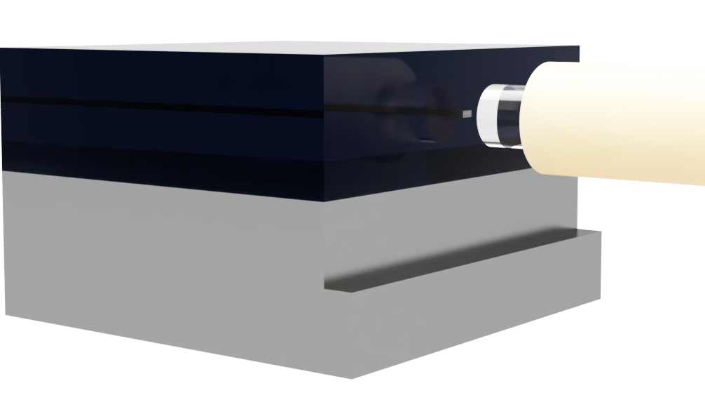
With the deep trench option, trenches 250 microns deep are etched along the perimeter of the chip to allow for edge-coupling with optical fibers. Silicon nitride edge couplers can be more efficient than silicon edge couplers due to the lower index contrast of silicon nitride and the increased thickness of our silicon nitride layer compared to the standard silicon device layer. Additionally, the thick cladding oxide and BOX layers in our silicon nitride platform allow for highly efficient edge couplers. Edge couplers are available in the NanoSOI PDK. The trench is patterned around an 8.78 x 8.78 mm enclosed area, centered on the submitted GDSII design. A deep-etch process is then used to etch through the cladding, silicon nitride device layer, buffer oxide, and through 250 microns of the underlying silicon substrate. The remaining silicon handle wafer is diced with a saw to separate the chips. The etch and dice process occurs on all four sides of the chip.
For more details about design of a deep trench layout, please see our deep trench design example.